Home » Without Label » Fermi Level In Semiconductor / With Energy Band Diagram Explain The Variation Of Fermi Energy Level With Impurity Concentration In Extrinsic Semiconductor Applied Physics 1 Shaalaa Com / (a) fermi level position in pure semiconductors at this point, we should comment further on the position of the fermi level relative to the energy bands of the semiconductor.
Fermi Level In Semiconductor / With Energy Band Diagram Explain The Variation Of Fermi Energy Level With Impurity Concentration In Extrinsic Semiconductor Applied Physics 1 Shaalaa Com / (a) fermi level position in pure semiconductors at this point, we should comment further on the position of the fermi level relative to the energy bands of the semiconductor.
Fermi Level In Semiconductor / With Energy Band Diagram Explain The Variation Of Fermi Energy Level With Impurity Concentration In Extrinsic Semiconductor Applied Physics 1 Shaalaa Com / (a) fermi level position in pure semiconductors at this point, we should comment further on the position of the fermi level relative to the energy bands of the semiconductor.. A semiconductor is a solid that is defined as having its fermi level (chemical potential) in a band gap of the electronic structure of the solid, which is not too large compared to the thermal energy, so that, according to the fermi distribution, at room temperature you have a significant number of electrons and/or holes in the conduction and. Intrinsic semiconductor, as seen in figure 4. For si withnd= 1015 cm3andni = 1010 cm3, using equation 3, ef nis 0.25evaboveef i. Of electrons in conduction band and no. Fermi level is the highest energy state occupied by electrons in a material at absolute zero temperature.
Whenever the system is at the fermi level, the population n is equal to 1/2. The fermi level is the surface of fermi sea at absolute zero where no electrons will have enough energy to rise above the surface. Fermi level of extrinsic semiconductor extrinsic semiconductors are formed by adding suitable impurities to the intrinsic semiconductor. Due to lack of sufficient energy at 0 kelvin, the fermi level can be considered as the sea of fermions (or electrons) above which no electrons exist. A semiconductor is a solid that is defined as having its fermi level (chemical potential) in a band gap of the electronic structure of the solid, which is not too large compared to the thermal energy, so that, according to the fermi distribution, at room temperature you have a significant number of electrons and/or holes in the conduction and.
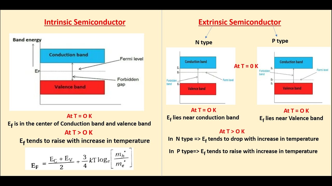
Conduction Mechanisms In Organic Semiconductors Springerlink from media.springernature.com Fermi level of extrinsic semiconductor extrinsic semiconductors are formed by adding suitable impurities to the intrinsic semiconductor. The electrical conductivity of the semiconductor depends upon the total no of electrons moved to the conduction band from the valence band. Intrinsic semiconductor, as seen in figure 4. What is fermi level in semiconductor? Semiconductor doping and higher temperatures can greatly improve the conductivity of the pure semiconductor material. Where is fermi level located in an intrinsic semiconductor:(a) right at the midgap (b) near midgap but close to conduction band (c) near midgap but close to. However as the temperature increases free electrons and holes gets generated. In a perfect semiconductor (in the absence of impurities/dopants), the fermi level lies close to the middle of the band gap 1.
If you can bring the fermi level high enough, then part of the tail will go over to the conduction band.
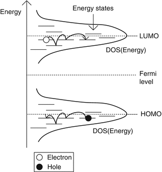
Fermi level in intrinsic semiconductor the probability of occupation of energy levels in valence band and conduction band is called fermi level. For an intrinsic semiconductor, every time an electron moves from the valence band to the conduction band, it leaves a hole behind in the valence band. Fermi energy of an intrinsic semiconductor. Fermi level is a kind of measure of equilibrium electronic energy of a solid material. In fact, this level is called the intrinsic fermi level and shown by e i: On semiconductors, the presence of surface states in the band gap is known to pin the fermi level position of the semiconductor. The fermi level plays an important role in the band theory of solids. Here nc is the effective density of states in the. Define fermi level in semiconductor at absolute temperature?fermi level is the highest filled energy level of electrons. Fermi level in extrinsic semiconductor fermi level in extrinsic semiconductor in extrinsic semiconductor, the number of electrons in the conduction band and the number of holes in the valence band are not equal. Of electrons in conduction band and no. E i = e c −e g/2 = e v +e g/2 (12) where e g is the bandgap energy. The electrical conductivity of the semiconductor depends upon the total no of electrons moved to the conduction band from the valence band.
However as the temperature increases free electrons and holes gets generated. Of holes in valance band are not equal. The term fermi level is mainly used in discussing the solid state physics of electrons in semiconductors, and a precise usage of this term is necessary to describe band diagrams in devices comprising different materials with different levels of doping. For si withnd= 1015 cm3andni = 1010 cm3, using equation 3, ef nis 0.25evaboveef i. Fermi level of extrinsic semiconductor extrinsic semiconductors are formed by adding suitable impurities to the intrinsic semiconductor.
Effect Of Temperature On Fermi Level Energy In Intrinsic Pure Semiconductor Youtube from i.ytimg.com Of electrons in conduction band and no. Kb is the boltzmann constant. Whenever the system is at the fermi level, the population n is equal to 1/2. Fermi levelis the state for which there is a 50% probability of occupation. Fermi level of intrinsic semiconductor. In fact, this level is called the intrinsic fermi level and shown by e i: For si withnd= 1015 cm3andni = 1010 cm3, using equation 3, ef nis 0.25evaboveef i. The fermi level represents the electron population at energy levels and consequently the conductivity of materials.
If you can bring the fermi level high enough, then part of the tail will go over to the conduction band.
Fermi level of intrinsic semiconductor. The fermi level is the surface of fermi sea at absolute zero where no electrons will have enough energy to rise above the surface. Fermi levelis the state for which there is a 50% probability of occupation. This definition of fermi energy is valid only for the system in which electrons are free (metals or superconductor), or any system. Due to lack of sufficient energy at 0 kelvin, the fermi level can be considered as the sea of fermions (or electrons) above which no electrons exist. In a perfect semiconductor (in the absence of impurities/dopants), the fermi level lies close to the middle of the band gap 1. On semiconductors, the presence of surface states in the band gap is known to pin the fermi level position of the semiconductor. Of electrons in conduction band and no. The fermi level and band gap in a solid largely determine its electrical properties. The added impurity is very small, of the order of one atom. For si withnd= 1015 cm3andni = 1010 cm3, using equation 3, ef nis 0.25evaboveef i. Kb is the boltzmann constant. At absolute zero temperature intrinsic semiconductor acts as perfect insulator.
For the intrinsic semiconductor at 0k, 1.1 0, indicating equal concentrations of electrons and holes. Ec is the conduction band. Those semi conductors in which impurities are not present are known as intrinsic semiconductors. The term fermi level is mainly used in discussing the solid state physics of electrons in semiconductors, and a precise usage of this term is necessary to describe band diagrams in devices comprising different materials with different levels of doping.
Fermi Level Pinning At The Semiconductor Interface Under Different Download Scientific Diagram from www.researchgate.net In extrinsic semiconductor, the no. For the intrinsic semiconductor at 0k, What is fermi level in semiconductor? In a perfect semiconductor (in the absence of impurities/dopants), the fermi level lies close to the middle of the band gap 1. The fermi level is referred to as the electron chemical potential in other contexts. For si withnd= 1015 cm3andni = 1010 cm3, using equation 3, ef nis 0.25evaboveef i. Fermi level lies in the midway between the valence band top and conduction band bottom of an intrinsic semiconductor, as shown in fig. Fermi level of intrinsic semiconductor.
In extrinsic semiconductor, the no.
The added impurity is very small, of the order of one atom. So at absolute zero they pack into the lowest available energy states and build up a fermi sea of electron energy states. Semiconductor doping and higher temperatures can greatly improve the conductivity of the pure semiconductor material. The fermi level is the surface of fermi sea at absolute zero where no electrons will have enough energy to rise above the surface. The density of electrons in the conduction band equals the density of holes in the valence band. Fermi level of extrinsic semiconductor extrinsic semiconductors are formed by adding suitable impurities to the intrinsic semiconductor. (a) fermi level position in pure semiconductors at this point, we should comment further on the position of the fermi level relative to the energy bands of the semiconductor. The electrical conductivity of the semiconductor depends upon the total no of electrons moved to the conduction band from the valence band. If the temperature will be maintained at. What is fermi level in semiconductor? The fermi level lies between the valence band and conduction band because at absolute zero temperature the electrons are all in the lowest energy state. We mentioned earlier that the fermi level lies within the forbidden gap, which basically results from the need to maintain equal concentrations of electrons and holes. Fermi level lies in the midway between the valence band top and conduction band bottom of an intrinsic semiconductor, as shown in fig.